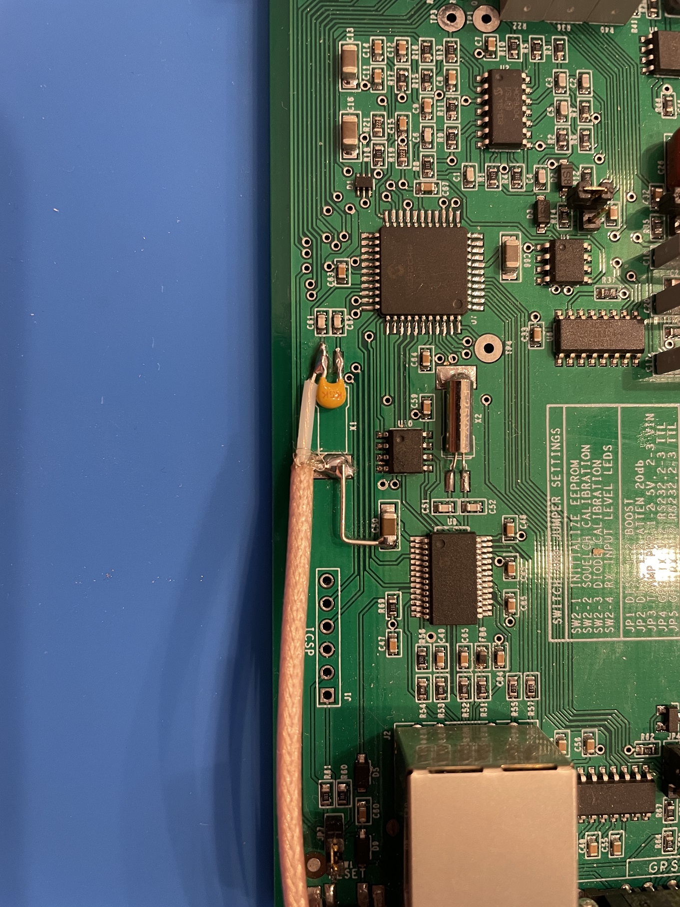
The Voter Board and RTCM use a 9.6 MHz crystal oscillator for the clock that times the DSPIC33FJ128GP802 (for the Voter Board) or DSPIC33FJ128GP804 (for the RTCM) processor. This clock becomes an issue when you try to simulcast with a PL/CTCSS tone using these devices. The PL/CTCSS tone is generated locally on the board which means that the PL/CTCSS tone frequency accuracy is dependent upon the accuracy of this crystal which is no where near accurate enough. The result is a pronounced "growl" on the air from the two PL/CTCSS tones being off frequency from each other. The question has been asked as to why the processor can't just use a 10 MHz input instead of a 9.6 MHz input. This question was answered by Jim Dixon himself and here is a quote from the AllstarLink Wiki Page.It comes down to timers and interrupts. In particular, the ADC servicing subroutine. With the way the dsPIC is configured with the 9.6Mhz oscillator, this subroutine is automatically called every 62.5uSec, as it is controlled by Timer 3 (TMR3). This subroutine is responsible for encoding the RX Audio Packets, and doing all the AtoD on the other analog inputs, RX Noise (for RSSI), Squelch Pot position, and Diode Voltage (temperature compensation). Every ODD time this subroutine is run, it encodes a RX Audio packet. Since this happens every OTHER time the ISR runs, that means it runs every 125uSec. Well, the reciprocal of 125uSec is 8kHz, so this is how we encode 8000 samples/sec of RX Audio! ***By default, encoding is ulaw, unless you SPECIFICALLY configure this client for adpcm in voter.conf ***Every EVEN time this ISR runs, it alternates measuring RX Noise, Squelch Pot Position, and Diode Voltage. So, each of those is measured every sixth time in, or every 375uSec. EVERY time this ISR runs, we bump some counters. Every time TMR3 expires, we service this routine and do an ADC conversion. We alternate between reading the RX Audio, and one of the other three channels (Squelch Noise, Squelch Pot position, and Diode (temp comp) voltage). So, as you can see, in order to encode ADPCM audio at 8kHz, we need precise timing to take the ADC samples of the audio and encode them. Because of this precise timing, and the restrictions in the clock dividers in the dsPIC, it works out that 9.6MHz is the most suitable (common) crystal/clock to use.
In short, we need to use 9.6 MHz for the processor. This presents a unique challenge that I overcame several years ago. When I first started my simulcast project, there wasn't anything readily available for a decent price that would produce an accurate and precise enough 9.6 MHz signal readily available so I had to create my own. Today however, There is a commercially available device that fits this bill. So if you don't wish to read about my homemade solution and just want to get it done (I don't blame you if you do) then the Leo Bodnar Mini GPS Programmable Reference Clock is for you. One word of warning with this device, the one I received had a small DC voltage on the output of the clock. This DC voltage destroyed the processor in one of my RTCM's when I was going to test it, I then needed to pull out my surface mount soldering skills to replace it (not fun). I used a .1uf ceramic capacitor in line with the Mini GPS unit to block the DC component and all was fine after that.
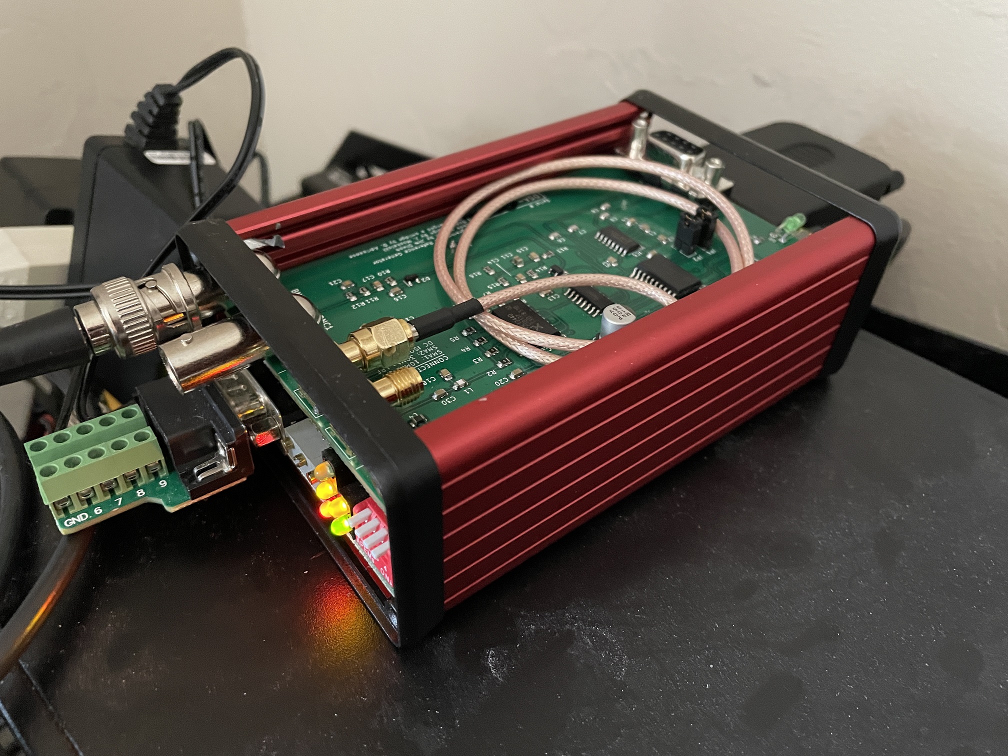
My home made 9.6 MHz PLL BoardThis is the board I first made to solve the 9.6 MHz issue. This works extremely well and I had plans on streamlining it and adding some features but there are a few reasons why I didn't. The main reason being that the Symmetricom OCXO that I found so plentiful on Ebay when I designed this board is scarce now. In reality, other voltage steerable oscillators can be used with little to no modification of the board. The other reason, as stated above is the availability of a reasonably priced, commercially available alternative that is more flexible. I continue to use these boards simply because I have a stockpile of parts to build them and they are easily repairable. The one small advantage this board has is that it can use an existing, onsite 10 MHz reference instead of a separate GPS antenna. Theory of Operation This device is fairly simple in its operation. This board compares two signals: 1. 10 MHz provided from a highly accurate source such as a GPS clock 2. A sample of the 9.6 MHz OCXO output These two signals go through buffer amplifiers and then wave shaping amplifiers that flat top both sine wave signals, this is done to make them more compatible with the TTL IC's they are being fed into. Both this signals (now square waves) get divided down to a common divisor, in this circuit it happens to be 100 KHz. These two 100 KHz signals are fed into a XOR gate that acts as a Phase Detector which outputs a 200 KHz signal. As the PLL circuit attempts to achieve phase lock, the pulse width of the 200 KHz square wave out of the XOR gate will vary its pulse width. Eventually the pulse width will find equilibrium and remain steady. The output of the XOR is buffered and filtered to produce a variable DC output voltage. The voltage can be manually offset by a pot to get the DC voltage within the locking range of the circuit. Lastly, this DC voltage is fed to the frequency control pin of the OCXO to adjust the output frequency of the OCXO. The frequency of the OCXO is slowly pulled into phase lock with the 10 MHZ reference and once phase lock has been achieved the DC control voltage will remain constant, only moving a little bit to compensate for the aging of the oscillator. When the board is first powered on it may take up to 10 or 15 minutes to achieve phase lock due to the OCXO warming up to operating temperature. If the board is power off and back on again in a short period of time, it will run through its phase lock cycle again. If the OCXO is already warm when powered back on, it will take considerably less time for phase lock to be achieved. Origins of this circuit Full disclosure, I did not come up with this circuit. The circuit I have built is heavily based on an existing circuit that was used in the High Stability Motorola MSF5000 stations. My contribution was that I changed the TTL logic to provide the correct frequency division, changed some component values and simplified the circuit to make it more compatible with the OCXO control voltage range and make sure all the components were commonly available. I also omitted most everything else that was not required for this to work in order to simplify the design. I know there are far more sophisticated ways that could have been implemented but my focus was to have something that worked and was easy to build with common components, the OCXO being the only exception. Initial Prototype and First Finished Board I built this whole circuit for the first time on a proto board. Once I got everything wired up correctly, worked out some bugs and mistakes of my own, the circuit worked just as I hoped it would. I confirmed that it indeed was precise enough using my old trusty Racal-Dana 1992 frequency counter using a separate external GPS locked reference. One issue that did arise was that if it was in the presence of a strong RF signal or an electrical spark in the area (one of them being the igniter for my oil furnace!) The circuit would lose its PLL lock and go through its lock cycle all over again. I attributed this to my haphazard wiring job on the proto board and moved forward with designing a PCB for the circuit. I figured that a PCB with much shorter leads and proper RF decoupling methods would be less susceptible to these issues and I was correct. When I built the circuit on my newly made PCB's they were less sensitive but still susceptible to those same issues. I decided to encase the entire board in an aluminum Hammond project box that was tied to the ground of the circuit. This completely solved the issue and I could practically run a 9 volt battery across a file with no issues to the circuit operation. If you wish to see my YouTube video on my prototype board, click here. Building the 9.6 MHz PLL Board This board is a simple double sided board using all through hole components. The board fits well into this die cast, aluminum project box. I have the boards produced by a company in China called PCBway due to their very reasonable cost, fast manufacturing and shipping. All the parts with the exception of the OCXO were purchased from Digikey. If you wish to build your own or make modifications to this design all of the information is available to download, use the link below: Download 9.6 MHz PLL Board Documentation package here The documentation package includes the schematics, parts list and gerber files to have the PCB's made.
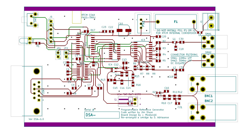
The Programmable Clock Generator Module (PCGM)
This was (emphasis on WAS) a device produced by Micro-Node International. The code it used was originally written by the original developer of Allstar, Jim Dixon WB6NIL (SK). What this device did was take a 10 MHz input reference and could output just about any frequency (square wave) from 6 MHz to 200 MHz by programming the unit using serial communication. Micro-Node ceased production of this device before I got started in this project so I was never able to get one. The firmware is publicly available on GitHub HERE and it's neat to take a look at. From what I have been told by those who do have these units, they were discontinued due to causing noise at the sites they were being used at. My theory is that this issue was caused by the square wave output which if you don't know, square waves are composed of odd order harmonics. These harmonics if let loose, can cause issues at a tower site.
Another Ham and I have recreated this unit and are making the information to make it publicly available.
I originally recreated the circuit and made the first PCB which I sent to a fellow ham whole took the whole project much further. This board uses the Microchip PIC part# PIC24FV32KA301 to interface and program the PLL chip ICS-307-02. You program the the PIC with the code found in GitHub from the link posted above using MPLAB IDE ver. 8.66.
This board outputs a single frequency on two different ports and is programmable from 6 MHz up to what the low pass filters will allow up to 200 MHz on each port. The values of L1, C18 and L2, C19 can be changed to whatever you need them to be.
DOWNLOAD - PRG and RTCM Case Complete Project Documentation
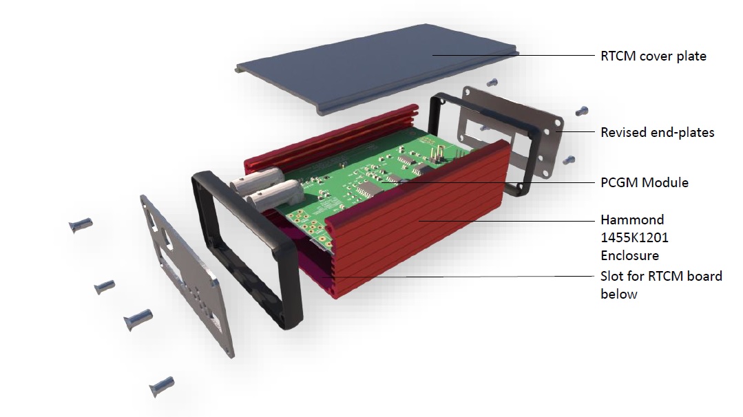
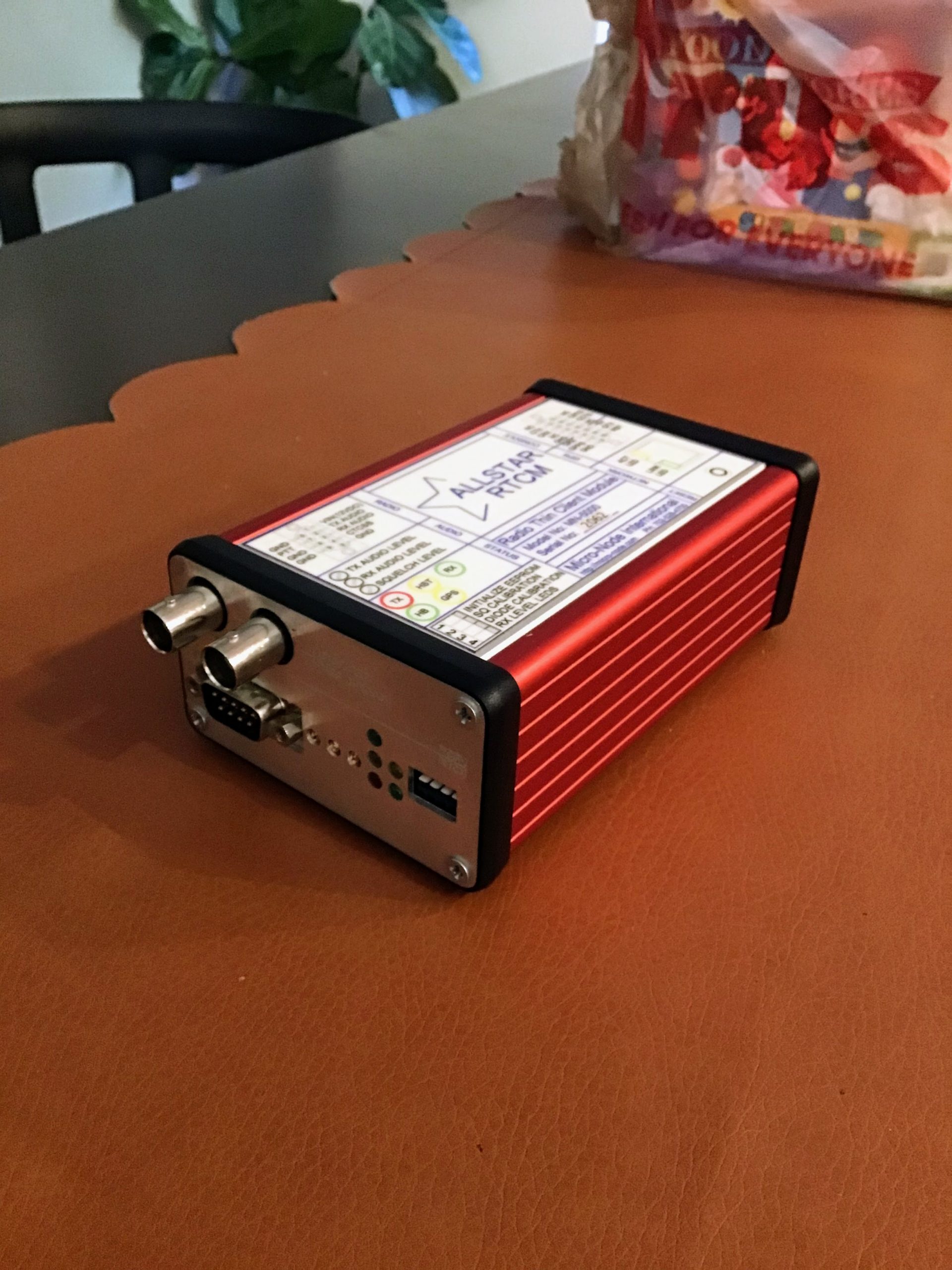
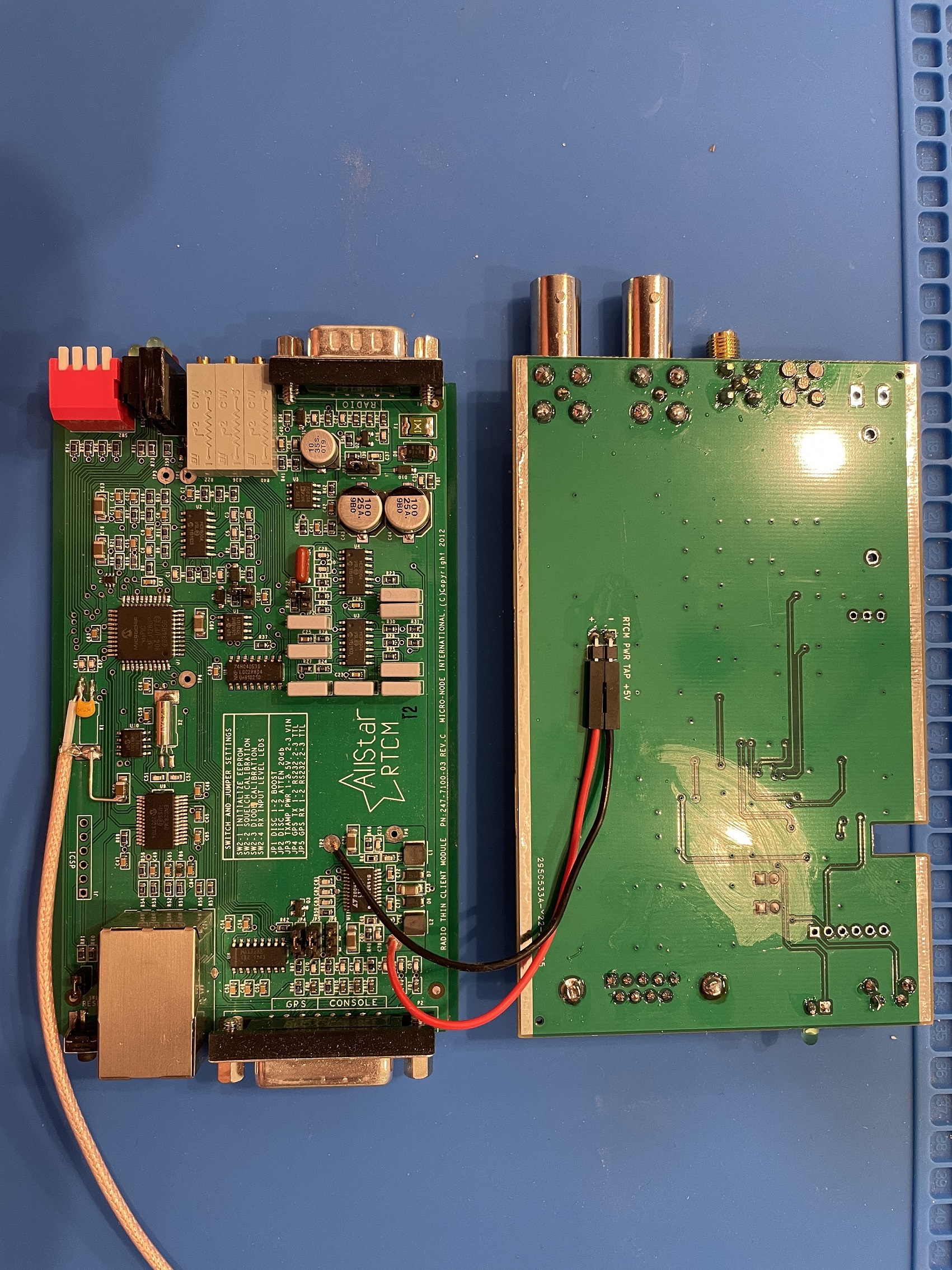
Here are some pictures of what this project is about, these pictures are from the ham who came up with the new case design and updated schematic.
QRP Labs ProgRock 2 Triple Programmable Output PLLQRP Labs Website for the ProgRock 2 This is a recent find that at this moment, is the smallest and cheapest option to get a GPS disciplined 9.6 MHz signal. I have one benched against one of my original PLL boards and it seems to hold true. The unit at the moment of my testing seems accurate enough once disciplined, for simulcast purposes as far as using it for our source of 9.6 MHz is concerned. This unit is a triple output programmable PLL device that also has the option to be GPS disciplined using 1PPS. Using the 1PPS input only allows you to use programmable outputs CLK 0 and CLK 1. Currently, I am designing and will soon be testing an adapter board using this unit in the new Radio Thick Client Module. UPDATE July 10th, 2023 Using the Progrock 2 has proved to be an excellent, cheap choice to provide the needed 9.6 MHz to the RTCM and Voter board. Along with the adapter I made for this to be used in the "Thick" Client Module, I have also created a complete GPS module designed around the Progrock 2 that can not only provide the needed 9.6 MHz, but also uses the second output of the Progrock 2 to provide a programmable reference signal for a simulcast transmitter. This unit also contains a GPS receiver that disciplines the unit as well. Right now, my device is still being tested in the field but is showing great promise. If you want to learn more about it, the link to the page is HERE. Once my testing is completed, I will offer completed units for sale and I will also post the parts list and gerber files to make the boards.
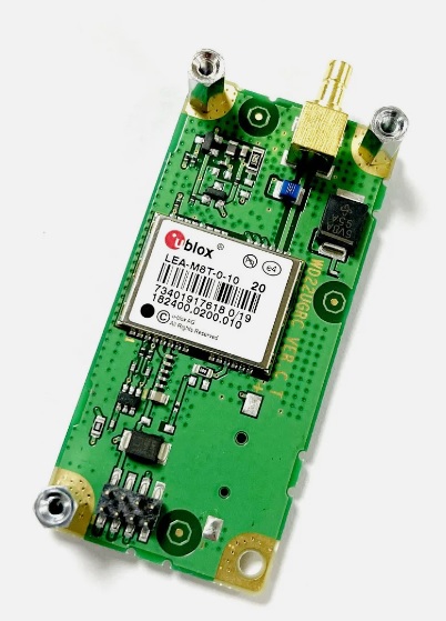
Ublox LEA M8T GPS Receiver Module
This module was something of a diamond in the rough I found. What makes this module a great find is that it has 2 time pulse outputs that are programmable from 1 Hz up to 10 MHz. Which means that with this unit alone, you can get the GPS NMEA data, 1 PPS and 9.6 MHz needed for the Thick Client Module. The big surprise is that at the moment of me writing this June of 2024, they can be had on Ebay for about $30 to $40.
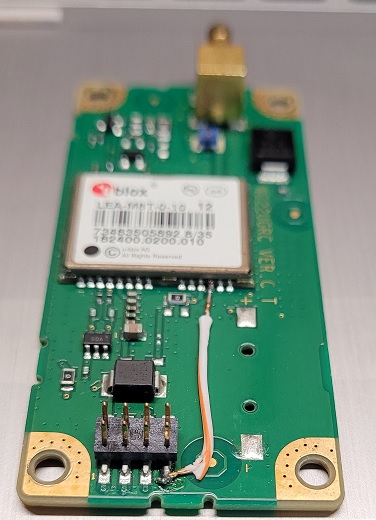
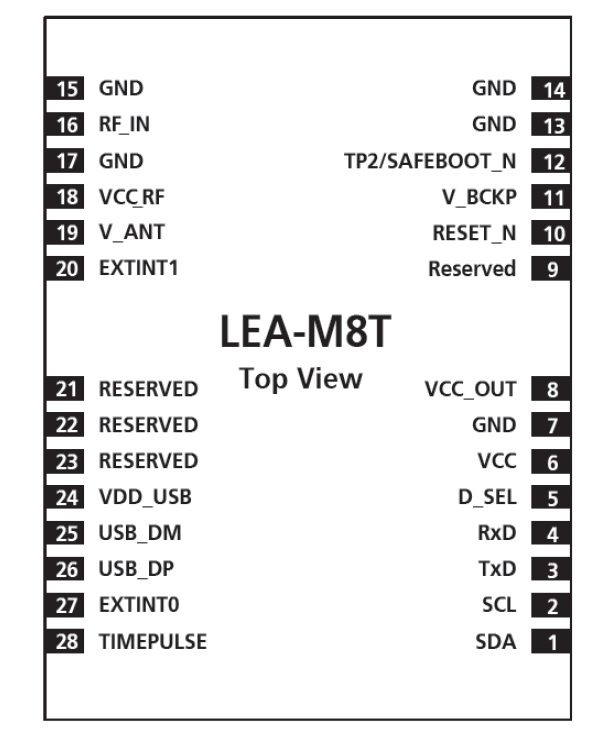
These boards on Ebay need only one small modification in order to do what we need them to do. These particular boards did not build out the second time pulse output, but this can easily be remedied by simply soldering a wire from the output on the GPS receiver unit on the board itself to the correct pin.
Ublox LEA M8T Complete Data Sheet Download
It does take a steady hand but it is not hard to accomplish. Once this is done, the second time pulse output becomes available to us for use for a 9.6 MHz reference to the Thick Client module. Once completed, the unit will need to be programmed with the Ublox Ucenter software in order to make it ready for service for our purposes. Here are screen shots of the settings that need to be changed and what they should be. Now in order to program this unit, you need a serial connection to it to. These units by default are Serial 9600 Baud, 8N1. The bare unit itself uses TTL levels for serial communication. So if you wish to power the unit up by itself, you will need a TTL to RS232 level shifter to communicate with it using a regular computer. The easier way would be to install it into the Thick Client Module first and set the jumpers to change the serial console port to GPS Data. That way, you can utilize the built in level shifter in the Thick Client Module to program the LEA M8T unit.
Here are the screen shots showing the settings that need to be changed.
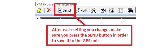
Note: you should hit the "SEND"
button after changing each setting in order to make sure it "sticks".
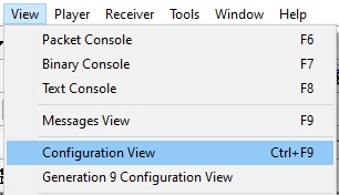
Go to Configuration view in the Ucenter software
Menu item: GNSS
Only leave "GPS" Enabled. The reason for this is because with the other GPS services enabled,
it changes the NMEA sentences coming out of the receiver and the Voterboard/RTCM/Thick Client module
cannot interpret them.
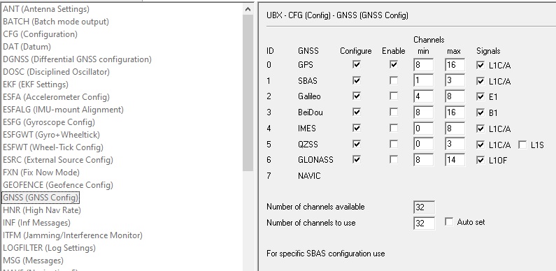
Menu item: TP5 (Timepulse 5)
Change Timepulse 2 settings to enable 9.6 MHz output, make sure duty cycle is set to 60%
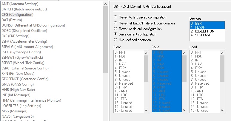
Menu item: CFG (Configuration)
Go to this page, make sure its set to "Save current configuration" and hit "SEND".
This will permanently write your changes to the non-volatile memory so your changes
aren't lost when you power the unit off and back on again.
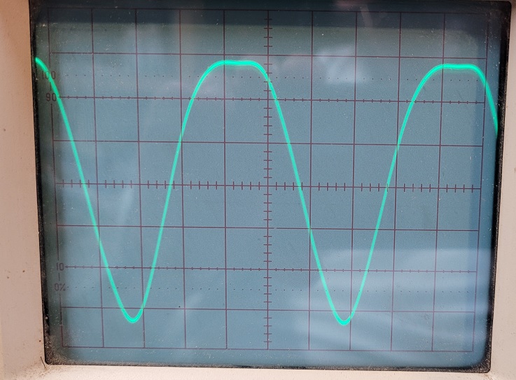
9.6 MHz Output Waveform
This should be the resulting waveform on the output of the Timepulse 2 pin.
This is the best I could get this waveform by playing with the duty cycle. 60% seems
to give the best results. This waveform is not critical since it is being used as a
clock for the micro controller and it accepts both sine wave and square wave inputs.
So, as you can see with a little bit of work we can get the 9.6 MHz we need for the Thick Client module on the cheap. The only thing we would need now for simulcast transmit is the appropriate GPS reference signal for a transmitter.
I neglected to mention about the Timepulse 1 setting. I did not mention it hear because that setting is already set to 1 PPS and really doesn't need to be changed in the context of what I am describing here. If you need to change it, you simple select "Timepulse 1" from the drop down menu on the TP5 (Timepulse 5) menu item and make your changes.
The waveform I am showing on this scope is going through a low pass filter which helps to clean up the
the square wave signal coming out of the GPS unit. The LEA M8T produces square waves for the time pulse outputs. When this GPS unit is inside the Thick Client module, it does not go through a low pass filter but it doesn't need to, to provide the 9.6 MHz clock needed to the PIC.